This is our goal.
It is optimized to be as easy to make at home as possible
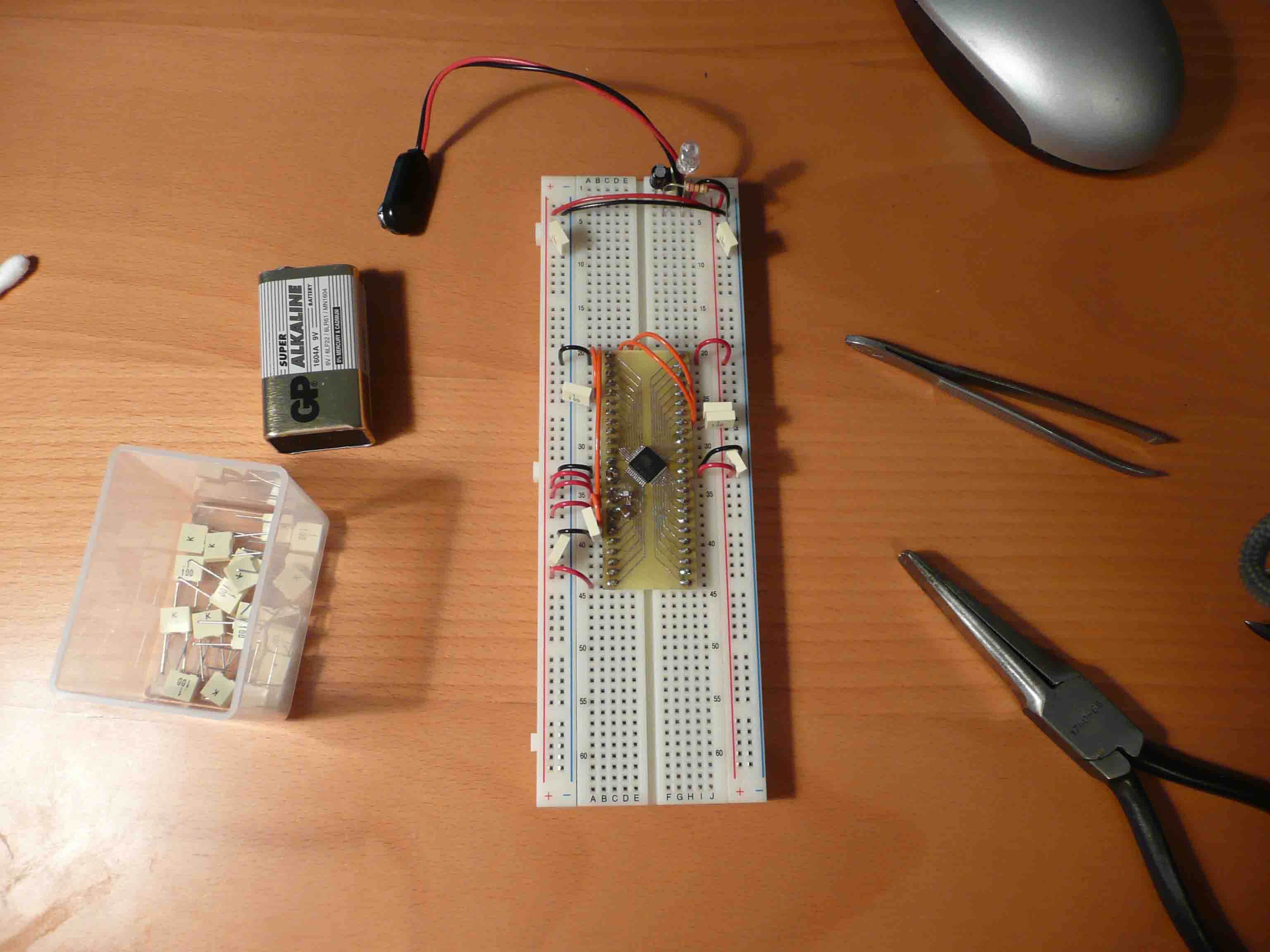
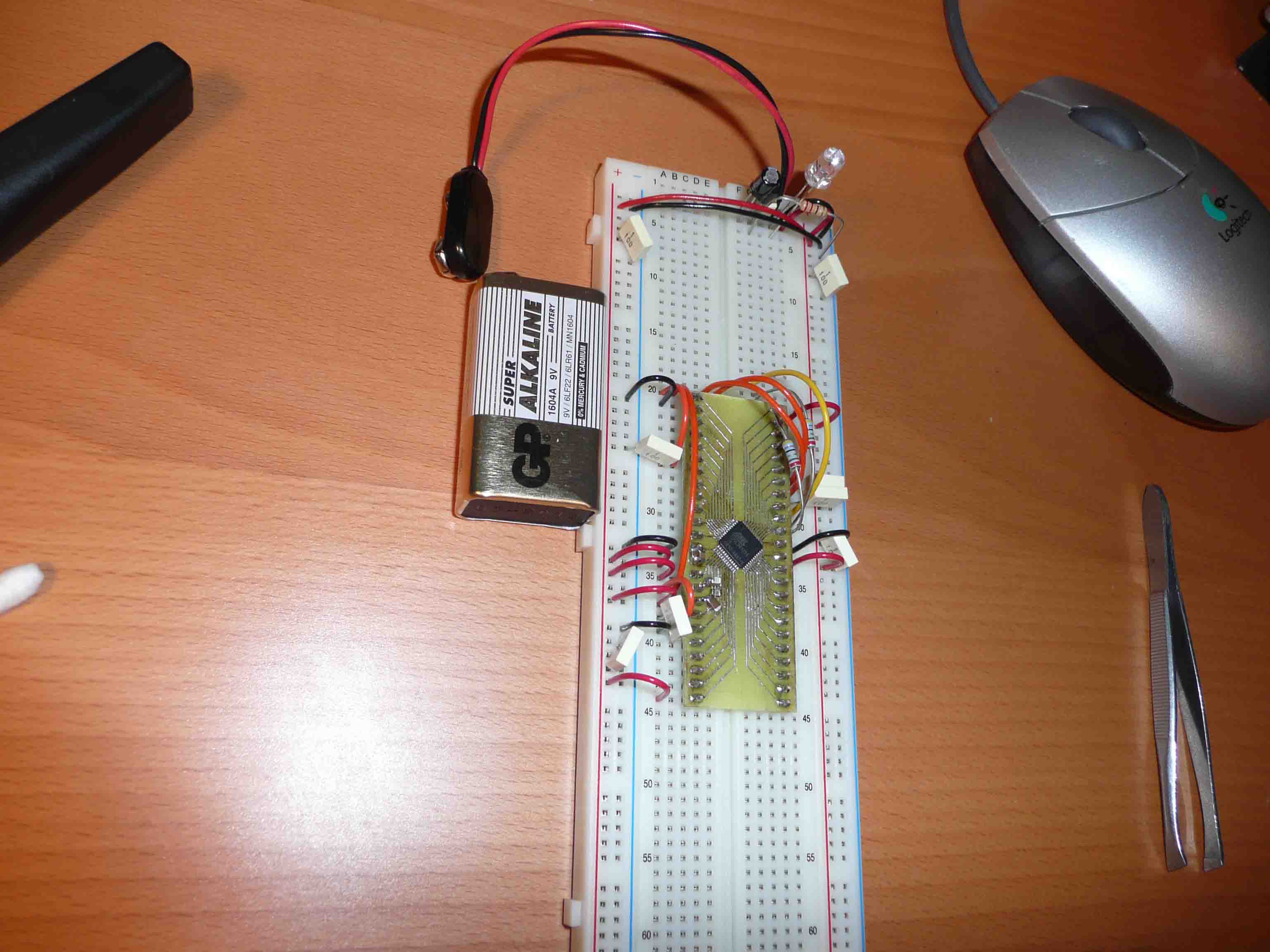
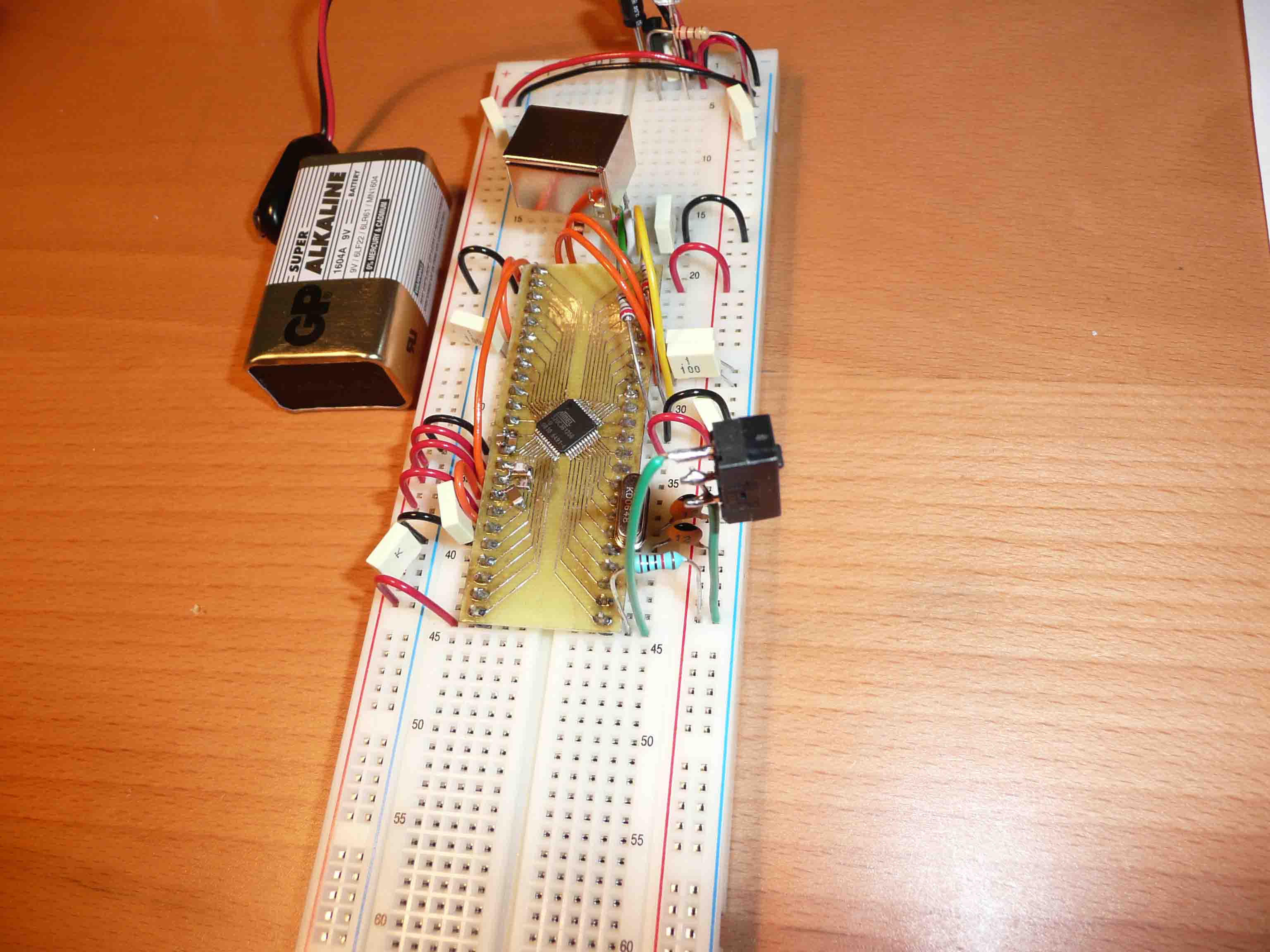
Schematics
We start with the most important, the Schematics, it is the same that are used for
the board you may buy:

Included are all the mandatory decoupling capacitors we need,
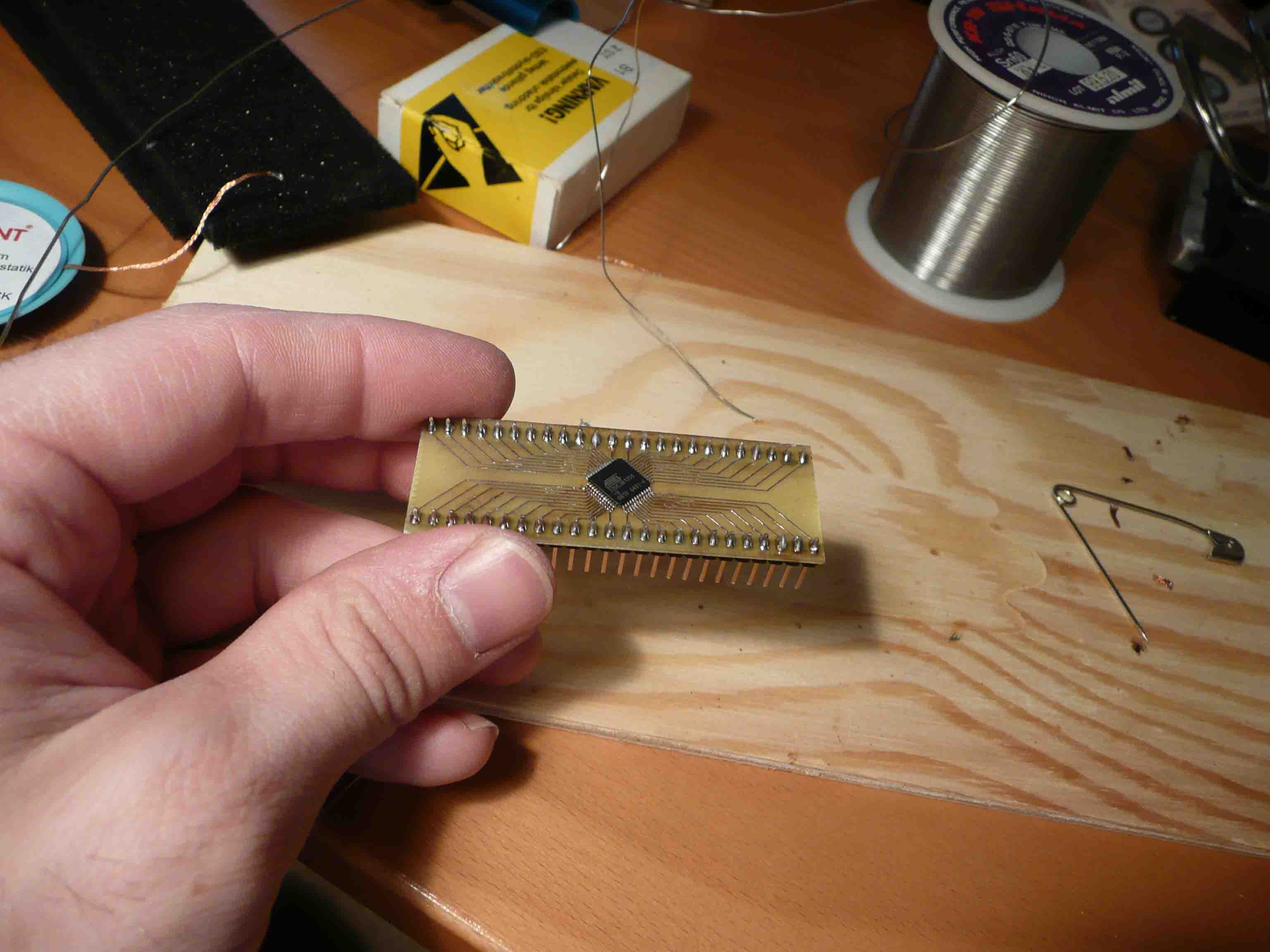
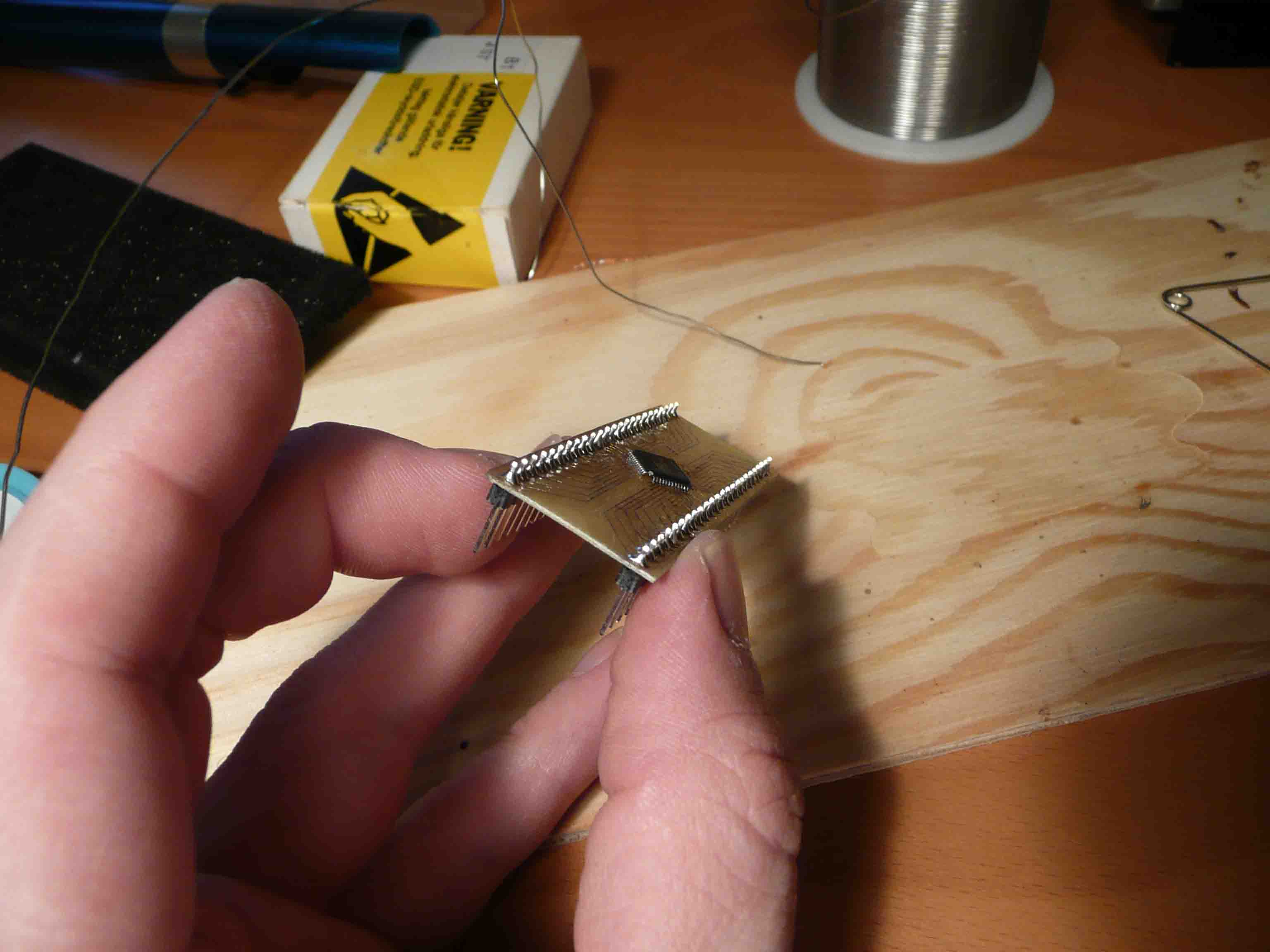
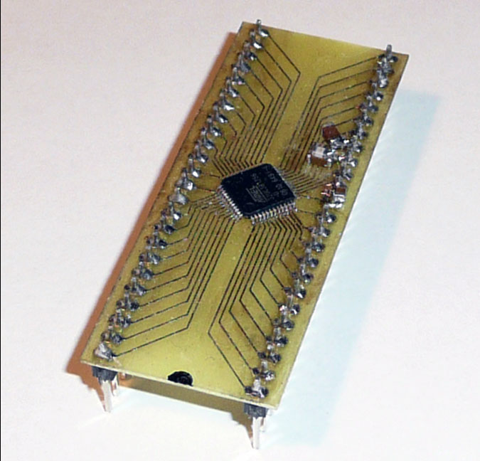
and how our DIL module should be connected. PIN-1 of the
AVR32 to PIN-1 of the DIL, PIN-2 to PIN-2 and so on.
And yes, we do need at least theese 14 capacitors.
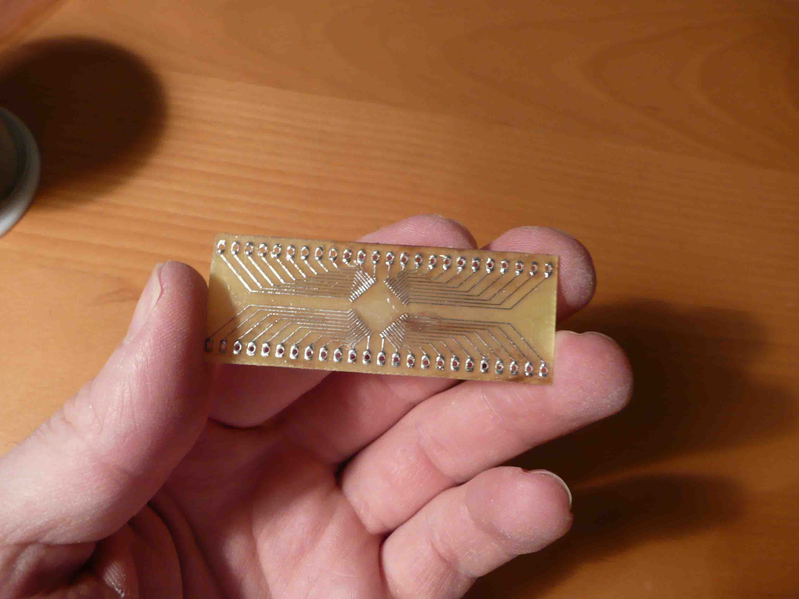
PCB design
If you want to try an other configuration, here are pointers to
documents to help your design:
- the UC3B Schematic
Checklist from Atmel
- Atmel doc: AVR32738 AVR32 AP7 Schematic Checklist (helps where the UC3B
is lazy).
- The EVK1101 reference design
- AT32NGW100 schematics
- The AVR32 UC3B doc has a lot info for hw construction: atmel.com doc32059.pdf,
we have pointed out that they have not properly mentioned the GNDANA in it.
It will be present in a later revision. Analogue GND is PIN-13 on the
AVR32UC3B1256.
- PCB Design Tutorial: www.alternatezone.com/electronics/files/PCBDesignTutorialRevA.pdf
- Design with as large distances as possible.
For 0.5 mm pitch, use first DRU 8 mil then DRU's for 10 mil and try to resolve as much as possible.
The rule is: If it is hard to fit it, first design with the manufacturers capabilities, then change to capabilities + 25%, and try to make everything or as much as possible pass this test.
- AVR32UC3B1256 MCU consumption: 23.5mA = all on @ 60 MHz
- AVR32UC3B1256 Max ratings total DC Output Current on all I/O Pin 200 mA
- 100 nF caps as close as possible to each supply-pin, avoid vias
- 3.3 uH 0.8A coil to the group of (1.8V) (A)VDDUSB , (A)VDDPLL,
(A)VDDOSC, 1.6A for the NGW100 (AP7000 MCU max 350mA IO+ 100mA MCU).
- uc3b: 3.3 uH to VDDPLL to help give a stable system clock,
3.3 uH to the group of VDDANA and ADVREF, or one 3.3 uH to each.
- 3.3 uH is equal to ~500 inch pcb-trace.
" If you use a 50-ohm trace on an FR-4 pcb, the inductance amounts to
about 7 nH per inch. This trace also has some parasitic capacitance,
but its value is negligible in this context."
- Do give MCU's power in a
Star-topology
- Bypass Capacitor
Sequencing How to do
powersupply lines, 2 plane old vs 4+ plane new
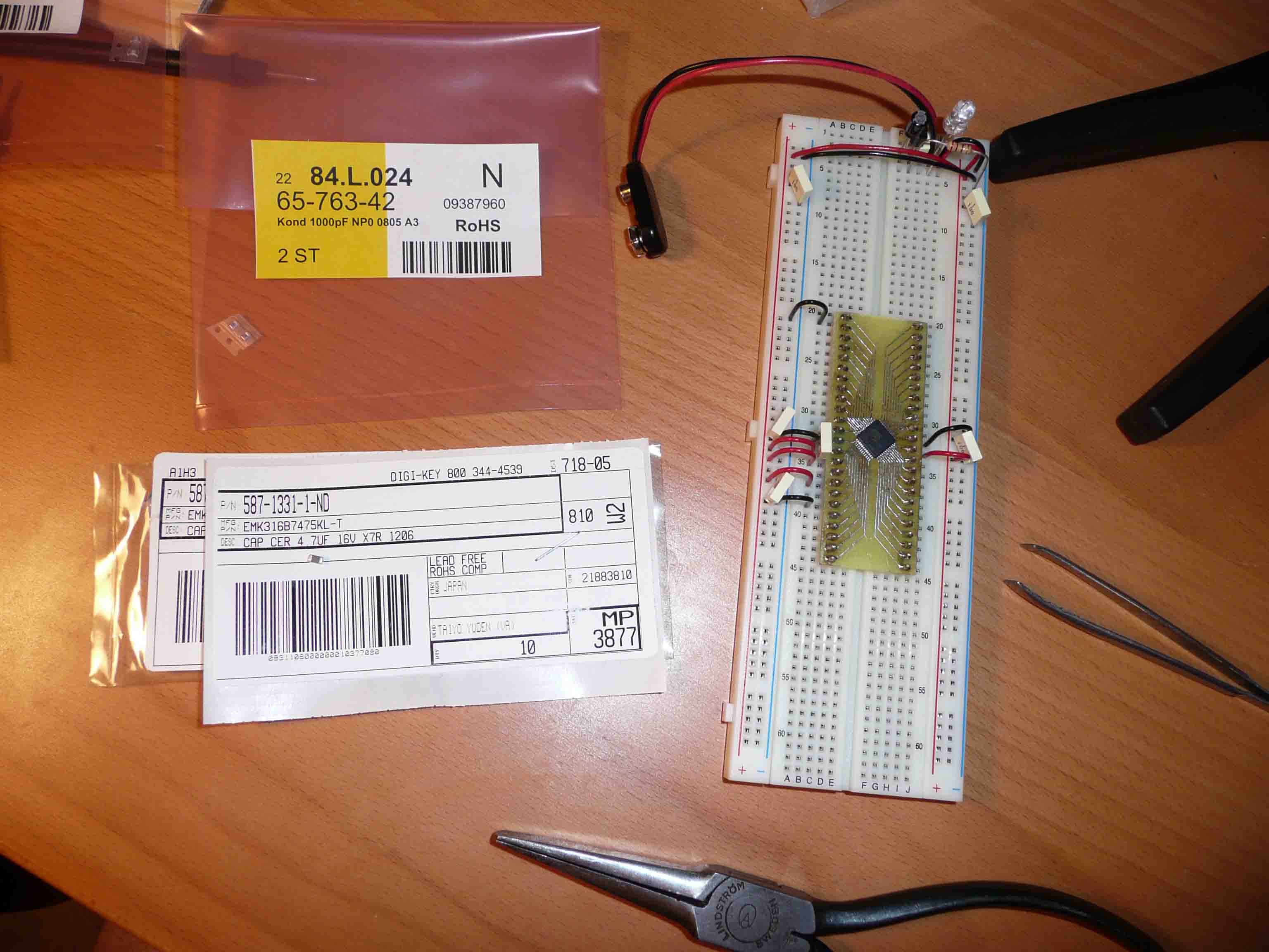
Notes: I only have one MPU on my board, that means I do not need to shield any
other components against GND or VCC noise, except incomming and outgoing from
my PCB.
We are in the 40 years old model: we got a CPU which uses power internally,
not only puts it on a bus
we also only have 2 planes.
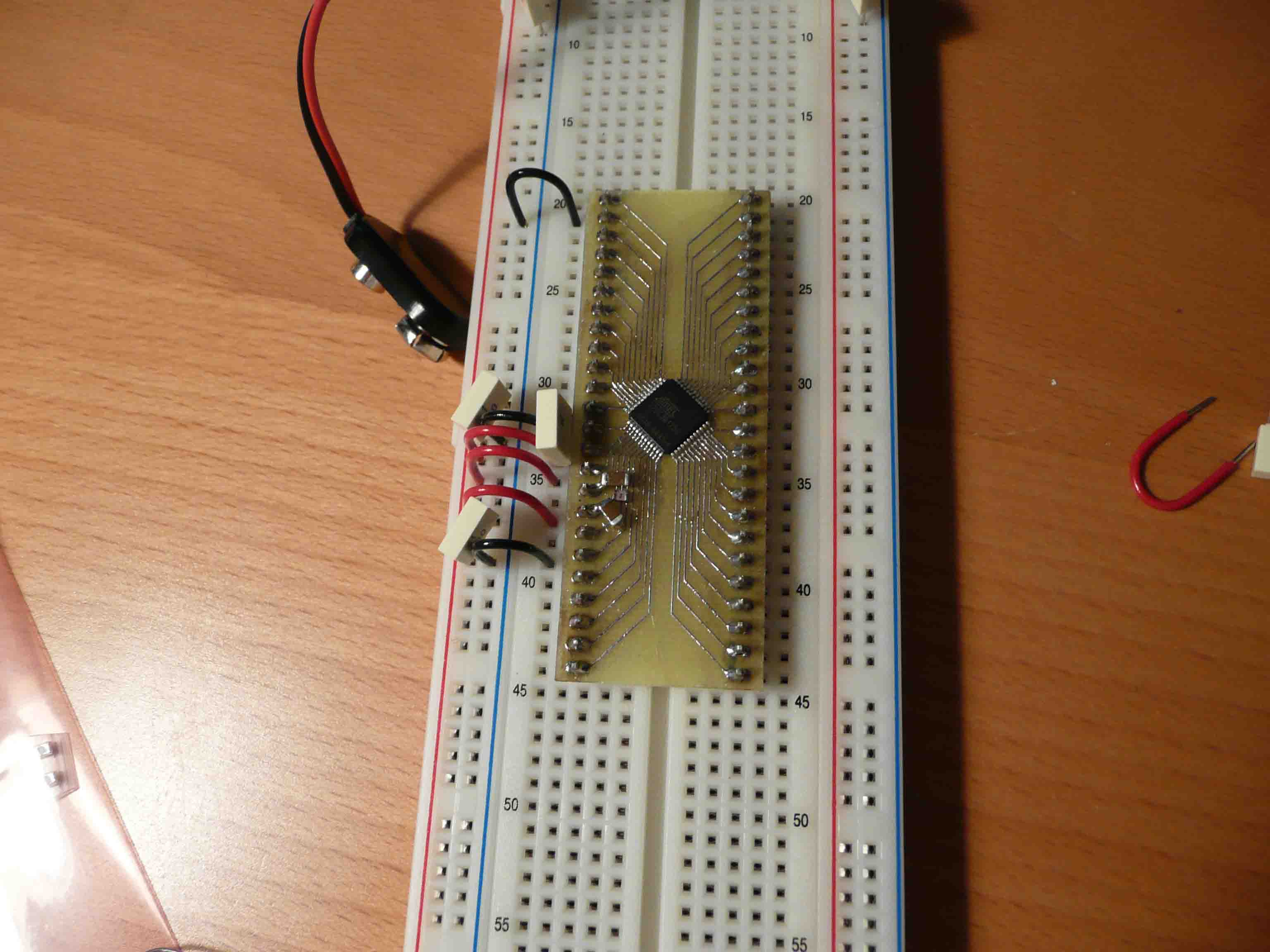
- Bypass Arrays
This arrangement reduces noise flow in both directions
Short lines from capasitors to supply-pins of the IC/MPU, longer from
capasitor to VCC supply rail. The longer lines acts as a coil, reduces noise.
But still focus on making them as short as possible.
Vias as close as possible to pin / chip GND and capasitors GND pin to the
GND plane.
- Here is a rule of thumb for power decoupling of nowadays digital electronics:
use capacitors in smallest package with largest capacitance + use dedicated power
planes in PCB and place them next and as close as possible to each other.
Obviously a designer must think about each design case separately as it
may require additional considerations. All of this stuff is actually an Ohm's law
From the PCB Design tut rev A
Some useful information and rules of thumb for high frequency design
- Keep your high frequency signal tracks as short as possible.
- Avoid running critical high frequency signal tracks over any cutout in your ground plane. This causes discontinuity in the signal return path, and can lead to EMI problems. Avoid cutouts in your ground plane wherever possible. A cutout is different to a split plane, which is fine, provided you keep your high frequency signal tracks over the relevant continuous plane.
- Have one decoupling capacitor per power pin.
- If possible, track the IC power pin to the bypass capacitor first, and then to the power plane. This will reduce switching noise on your power plane. For very high frequency designs, taking your power pin directly to the power plane provides lower inductance, which may be more beneficial than lower noise on your plane.
- Be aware that vias will cause discontinuities in the characteristic impedance of a transmission line.
- To minimise crosstalk between two traces above a ground plane, minimise the distance between the plane and trace, and maximise the distance between traces. The coefficient of coupling between two traces is given by 1/(1+(Distance between traces / height from plane)^2))
- Smaller diameter vias have lower parasitic inductance, and are thus preferred the higher in frequency you go.
- Do not connect your main power input connector directly to your power planes, take it via your main filter capacitor(s).
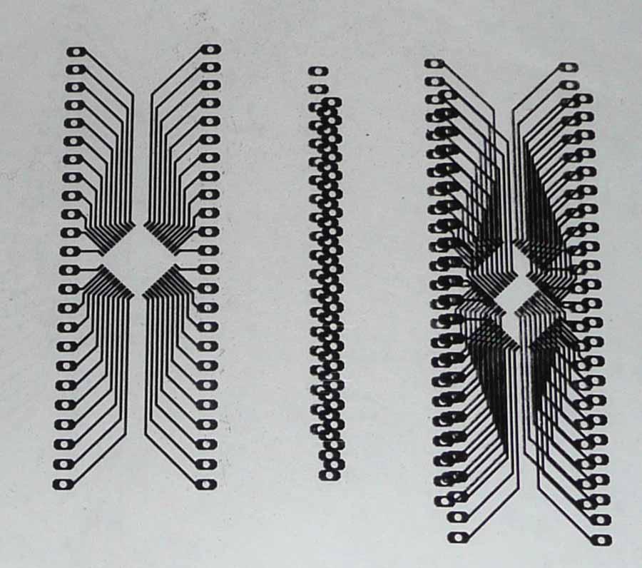
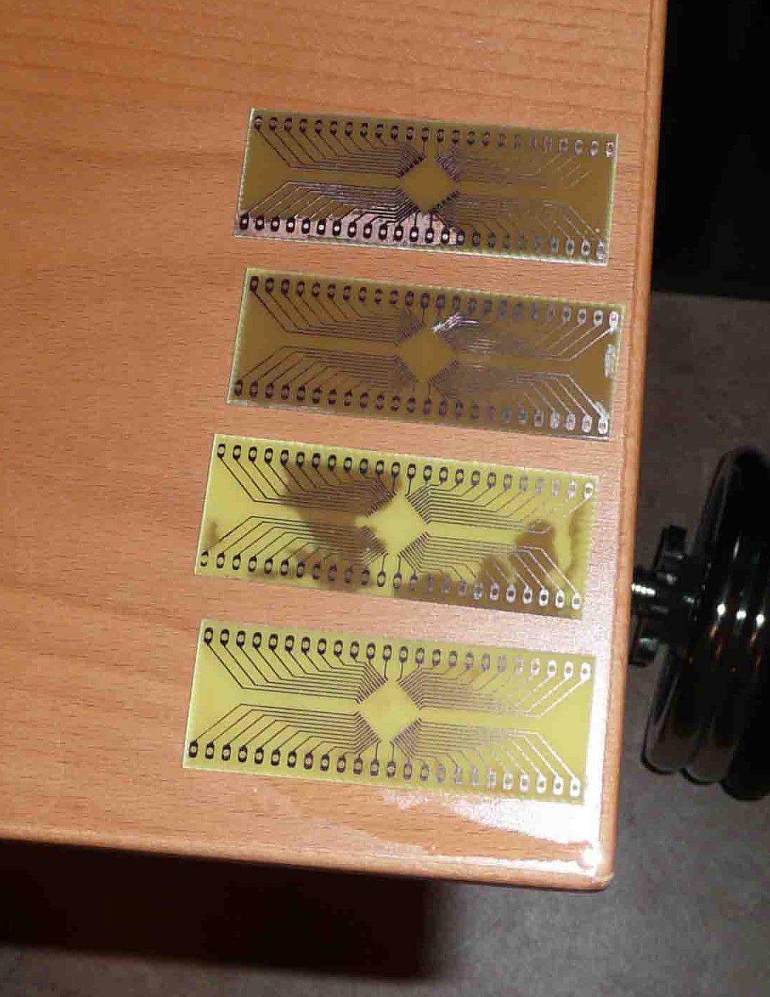
Ready to use pattern for the Transparent film
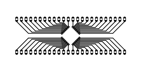
Just click on the image to download a PDF in A4 format for the PCB traces.
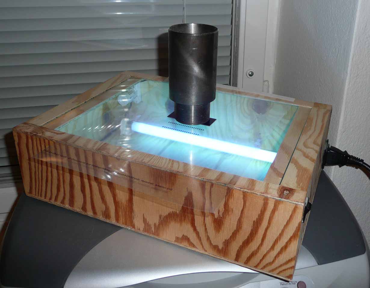
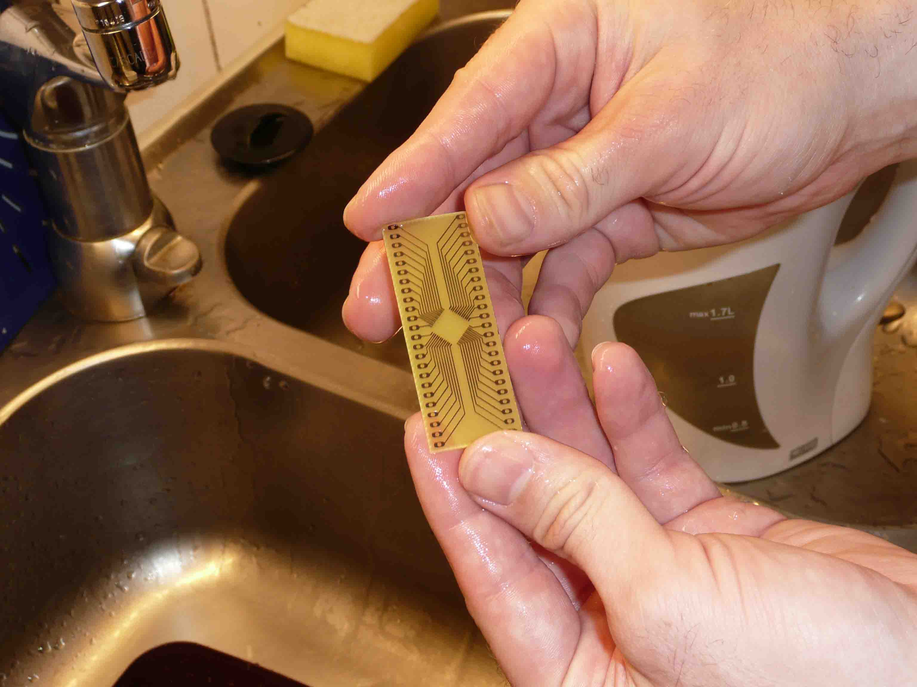
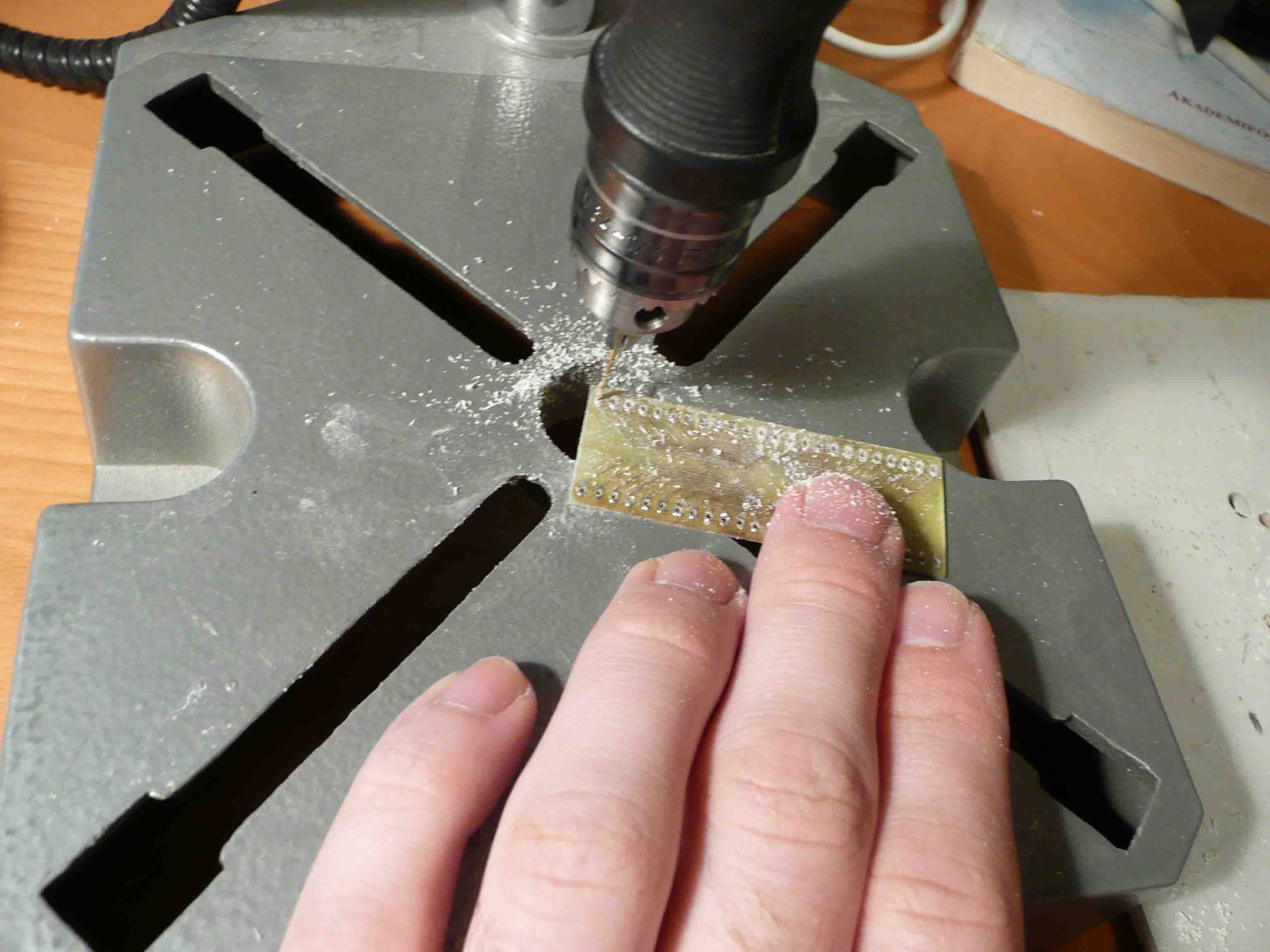
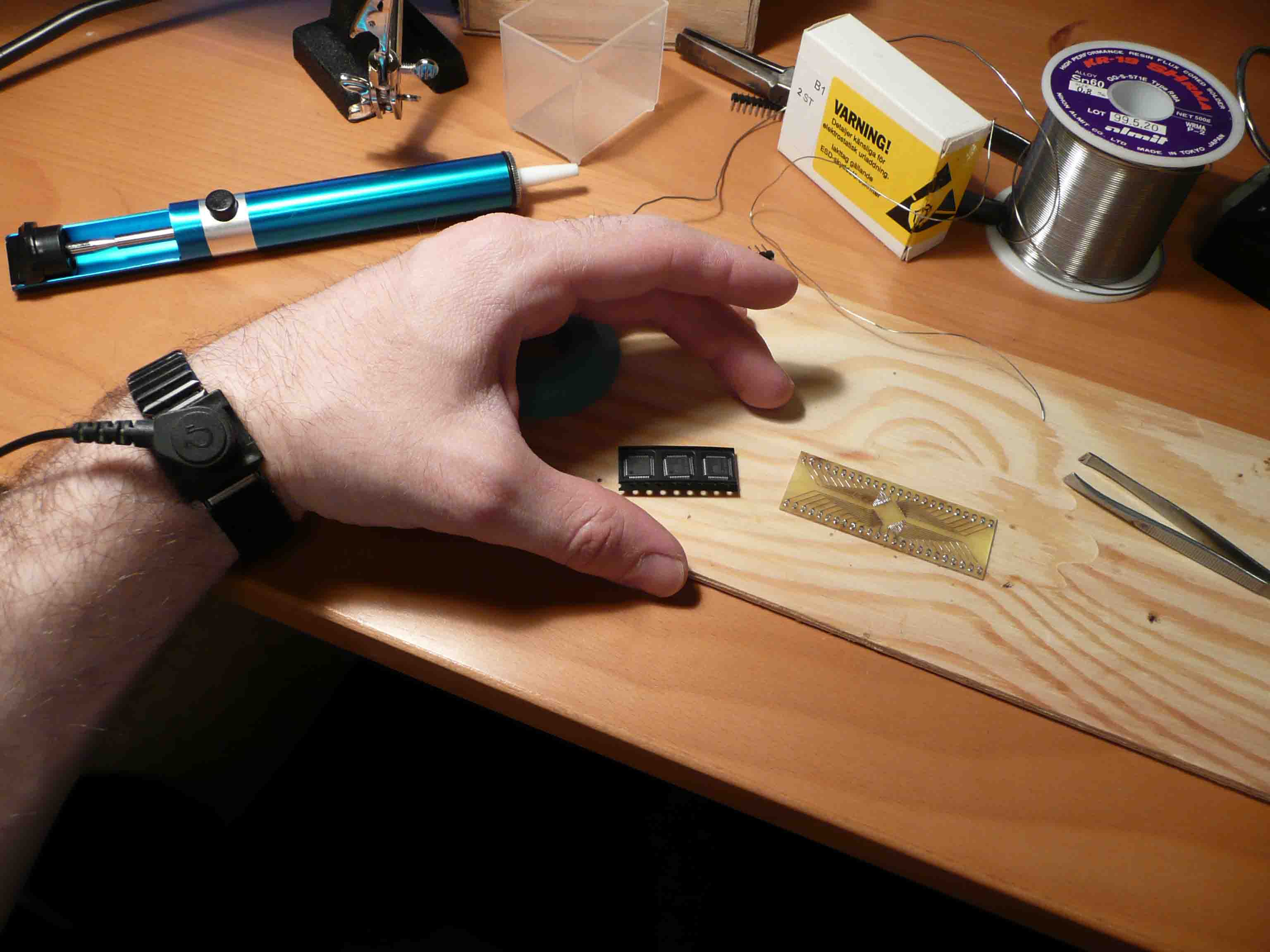
PCB Manufacturing at Home My Experiences
- The traces of the PCB will not be more well defined then the developed
photoresist, which will not be more sharp then the exposed photoresist,
which will not be more sharp then the patterns on the transparrent film,
which will not be better then your printer can deliver, which will
not be better then your CAD software can deliver, which will not be
better then you can deliver. Please keep up the quality / crispiness
during each step of your design chain. If your eyes think something is
fuzzy, or strange, then it is!
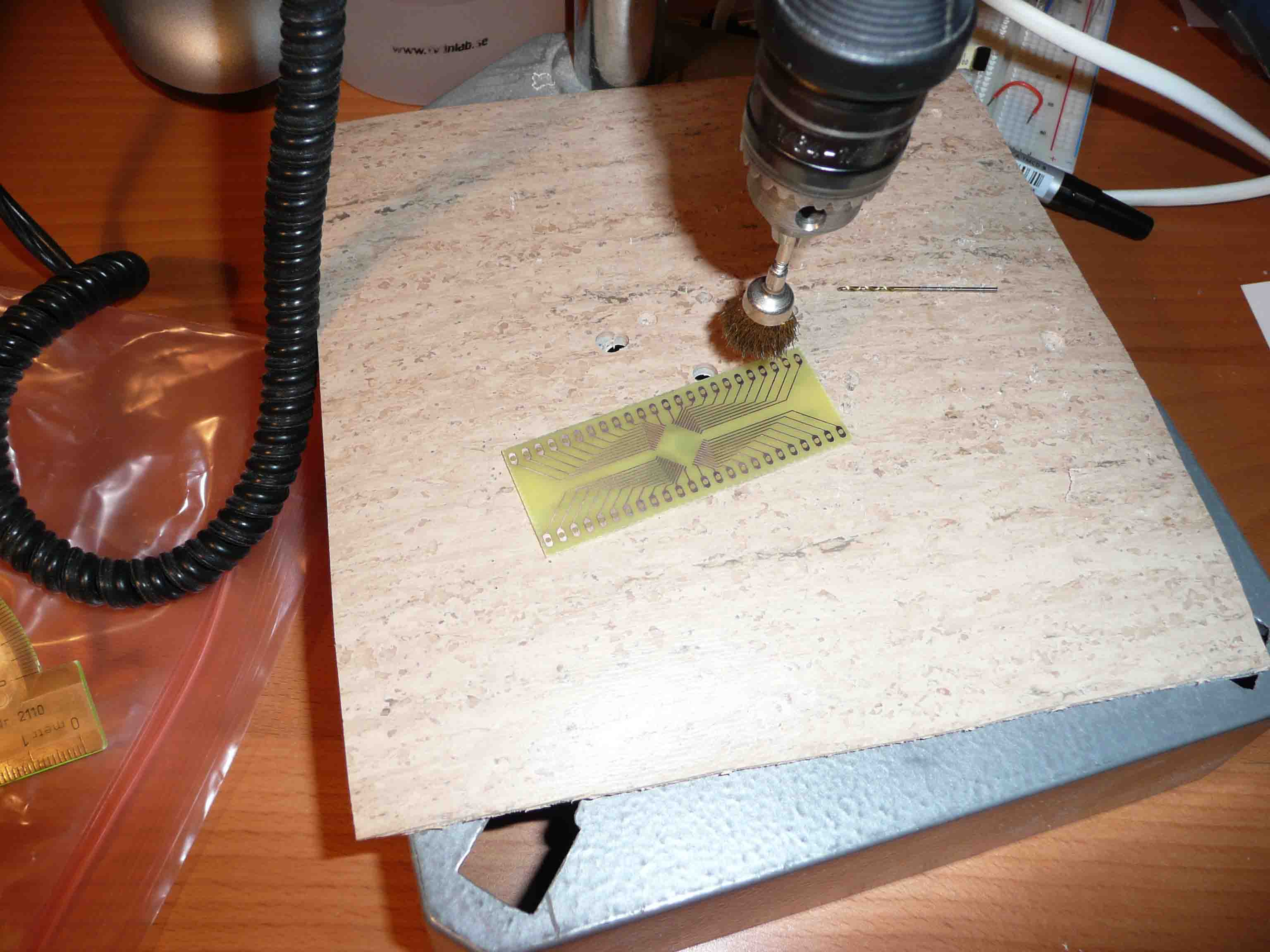
- Print on your best printer ("my" hp laser w coalpowder)
- Use heat resistant transparrent film, or the printer will be sad.
- When you inspect the pattern on the film, it should look well defined, no smear and clearly transparrent or black areas. Inspect finepitch-areas turned 0, 45 and 90 degrees if there is any. Most printers will give different quality on lines in different angles (orientation) on the film.
- Test your UV-bench for best exposuretime (my best ~10 minutes)
- Put weights on the laminate, to force it down against the film.
- The exposed laminate should have clearly defined lines, if fuzzy you have made some kind of exposure error.
Common ones: transparrent film not held against PCB, bad print on transparrent film, printing done on the wrong side of the transparrent film (it should be printed mirrored, with the print on the side of the laminate). To short or to long exposure. Printer ink not blocking the UV light enough (I use coal ink).
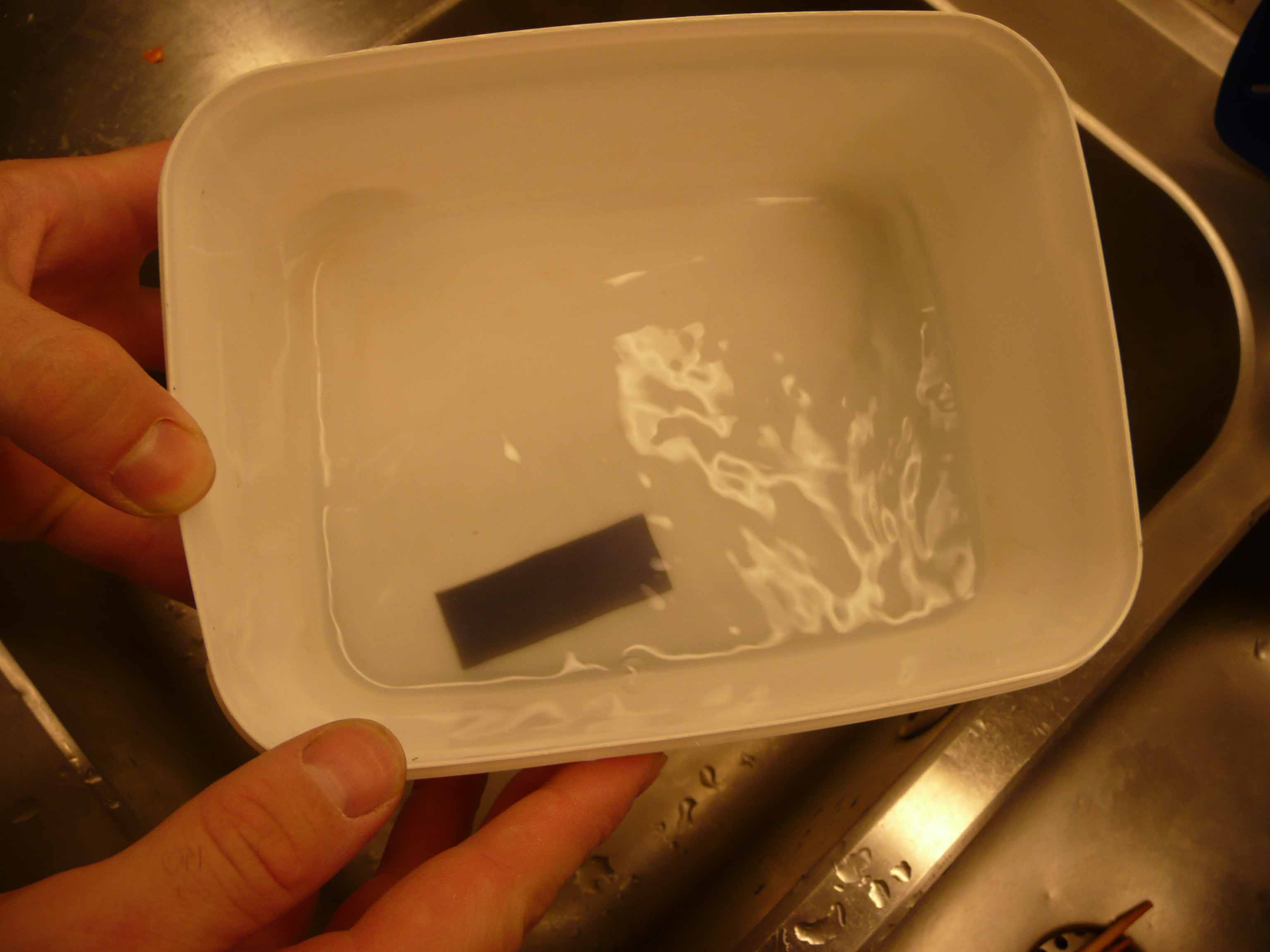
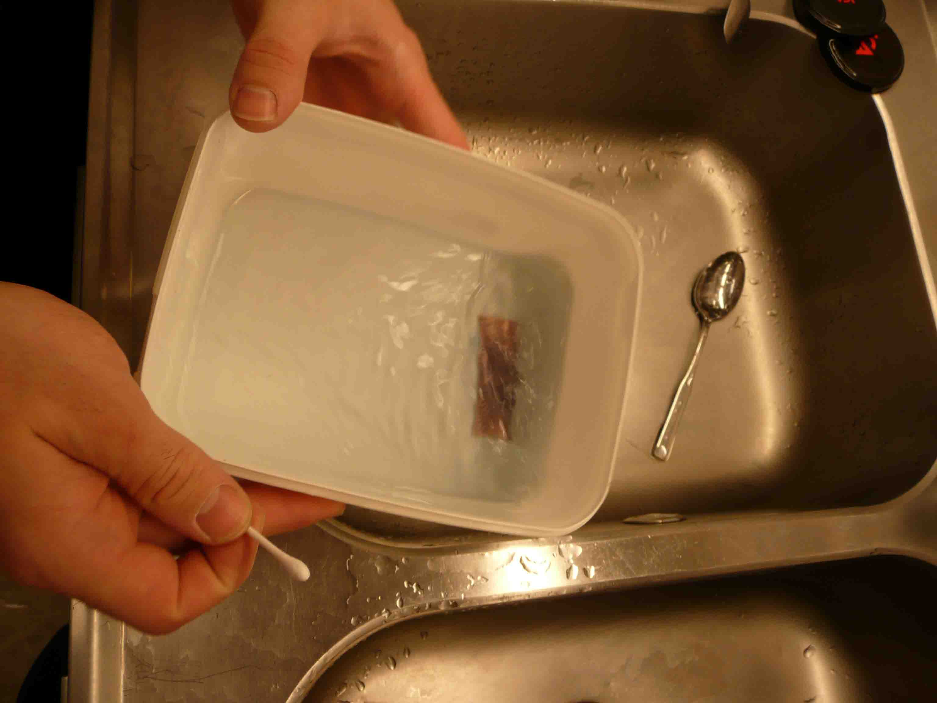
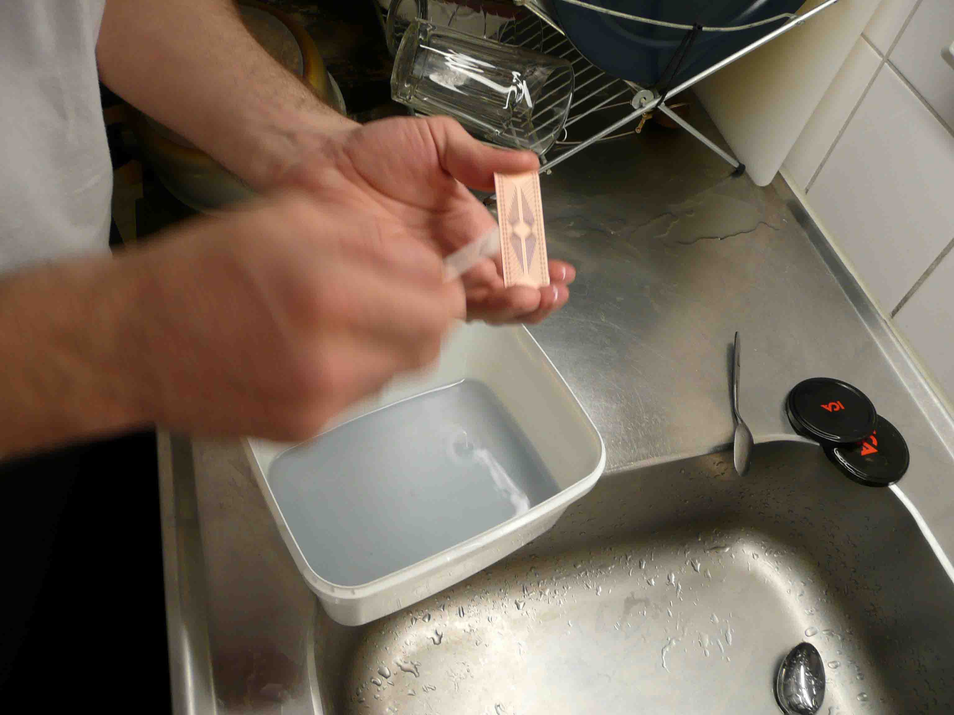
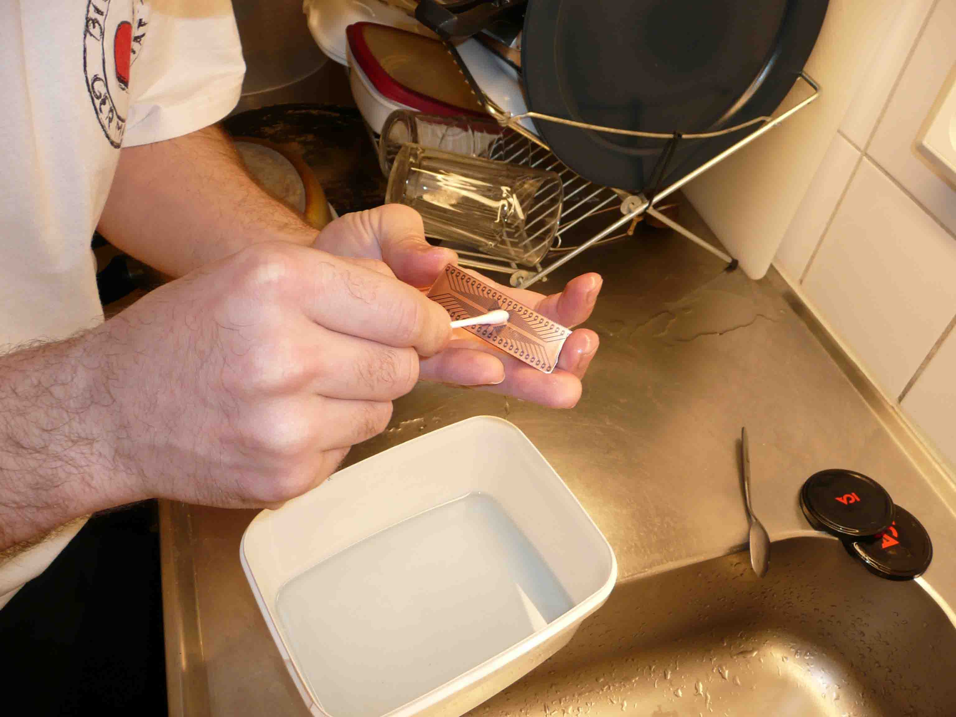
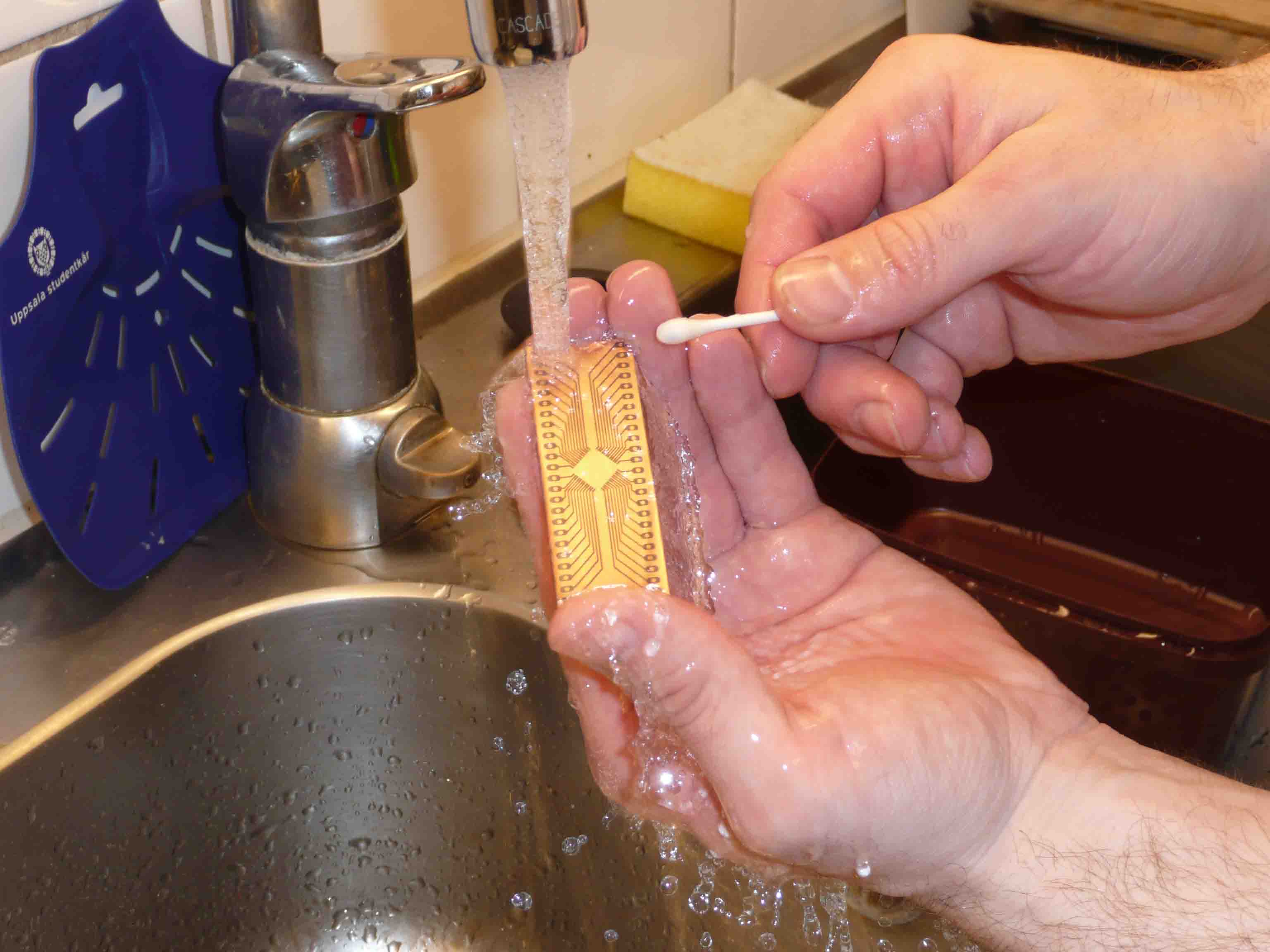
- Develop in 15-30 deg C NaOH solution, for 30-90 seconds. Please remember to wash asap, if you get any on you. I did not feel it at first once, but the next day I got a wound on my cheek!
- Use a tops to gently rubb/swabb the exposed laminate surface after 30s, and then again later if development was not finished. This helps a _lot_, it will create a much more defined PCB-pattern.
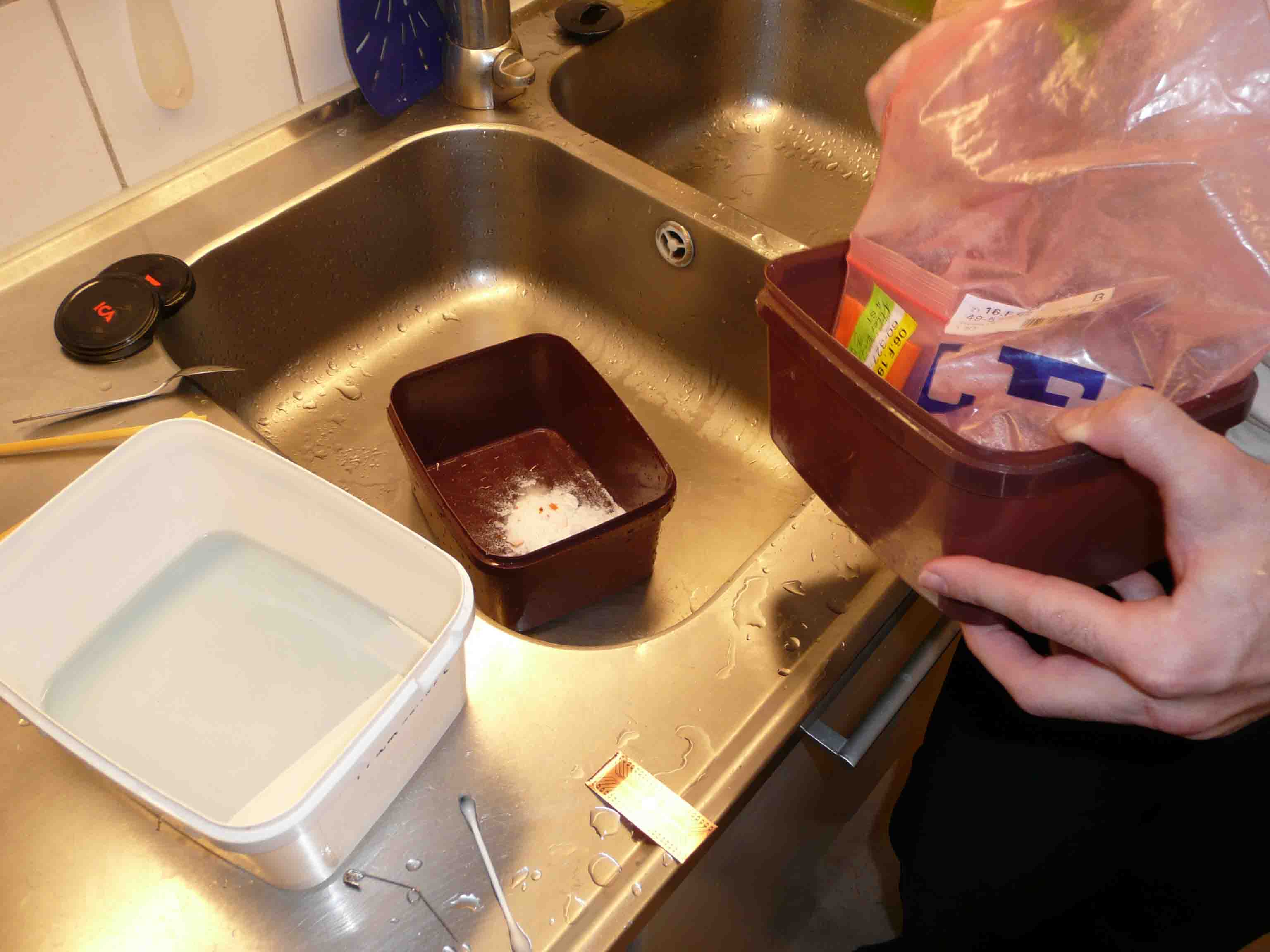
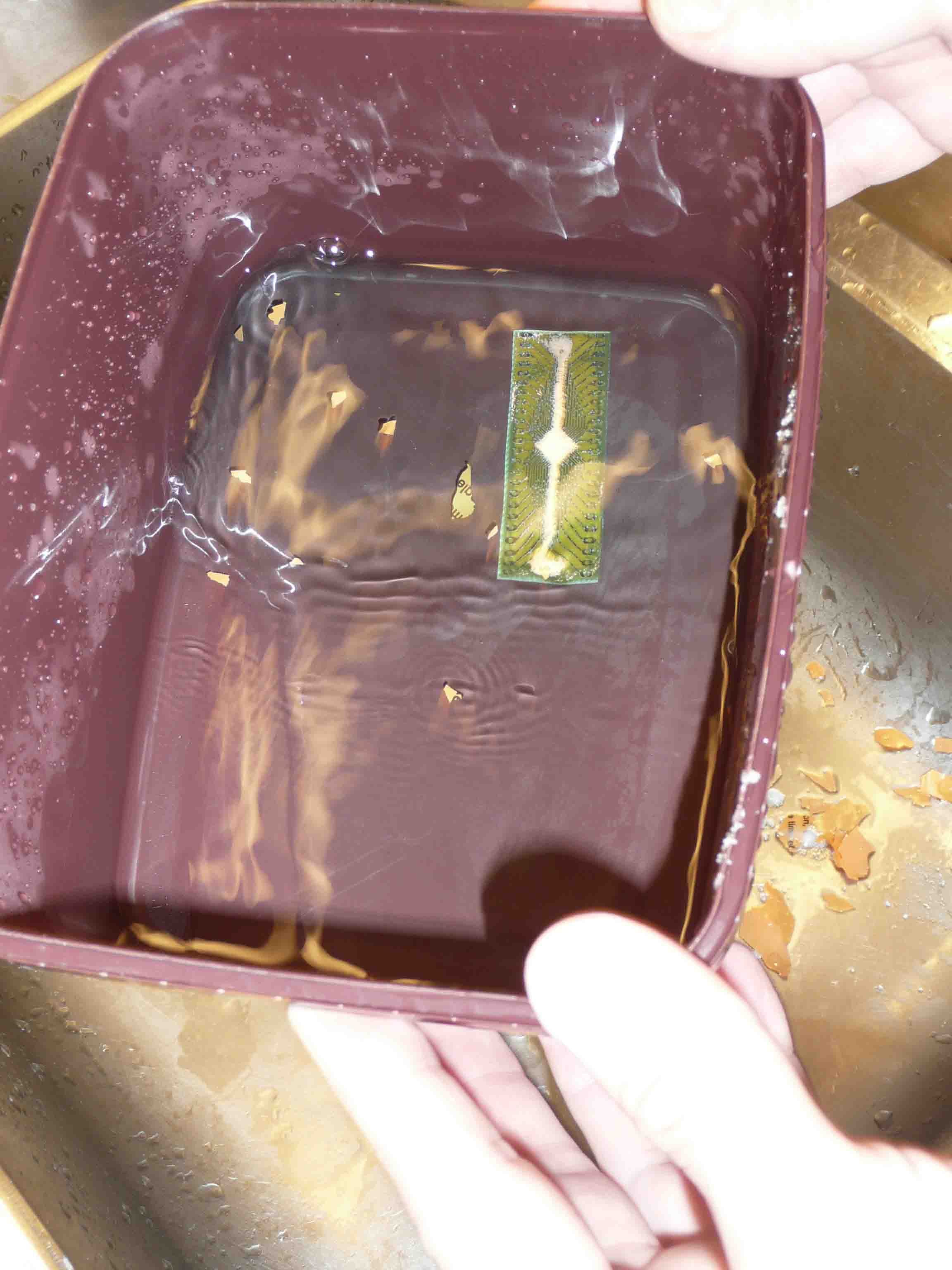
- Etch with stirring, to avoid boubles to stick and stay on the surface.
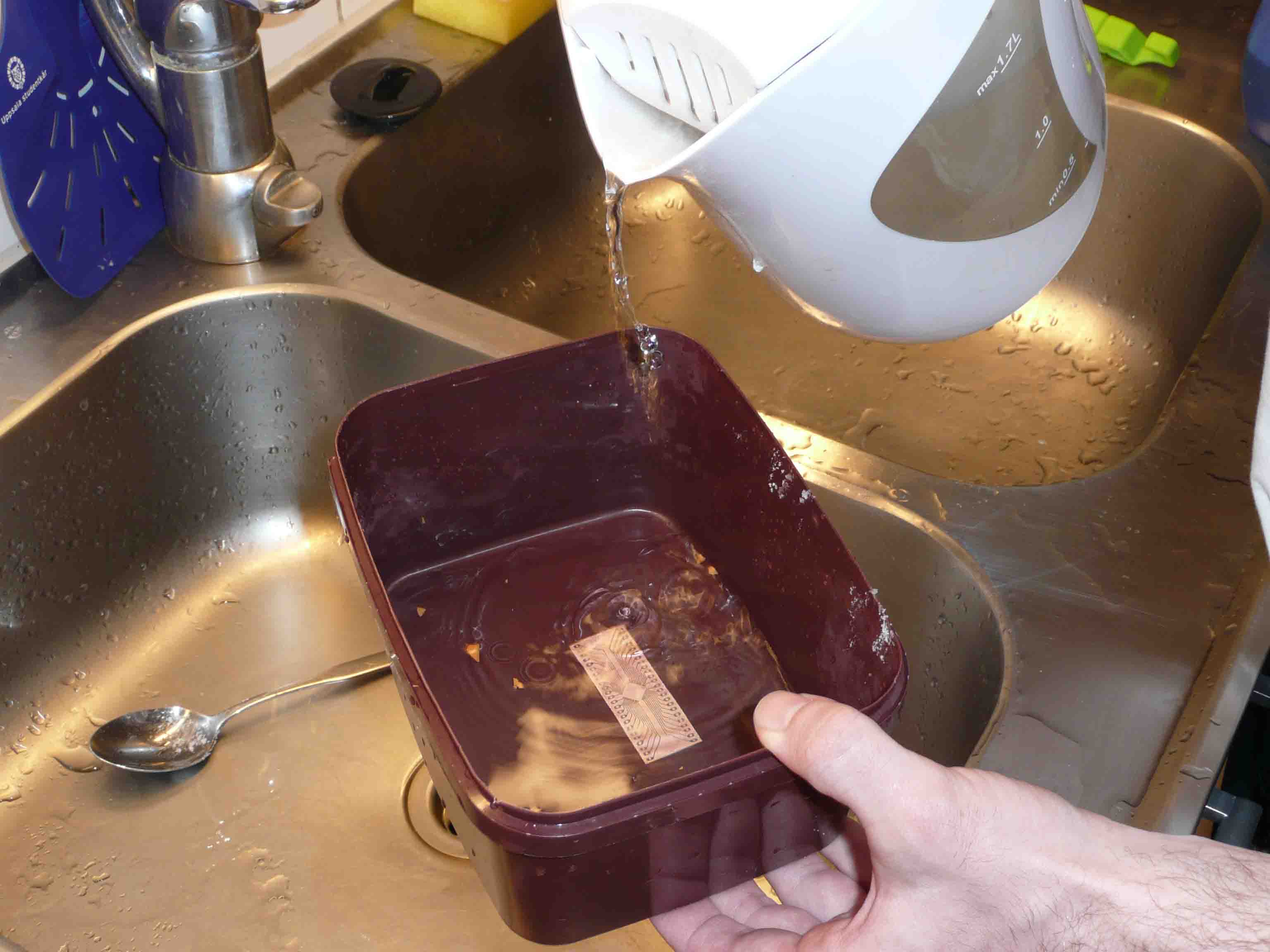
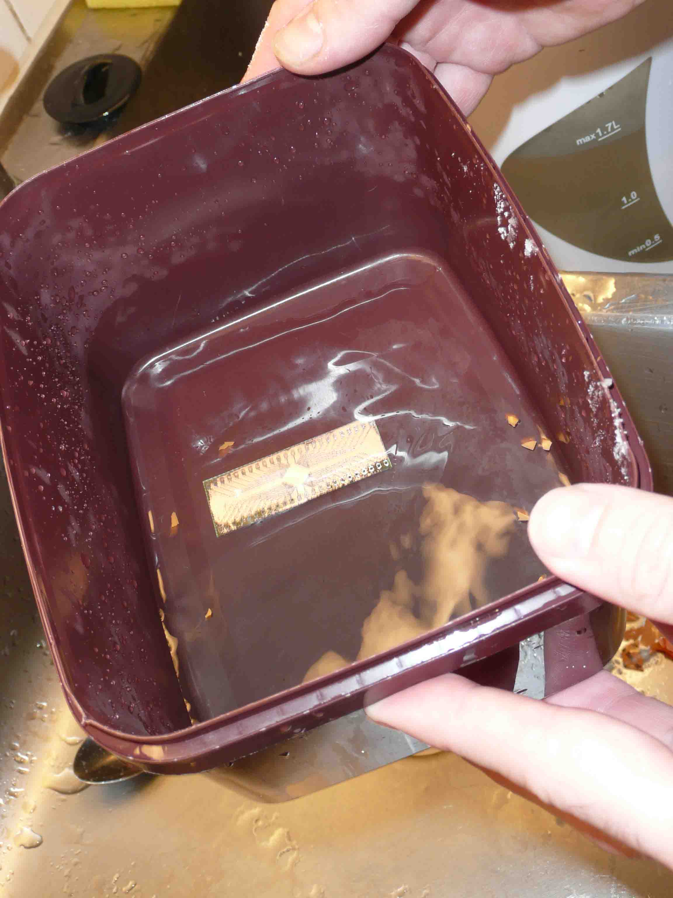
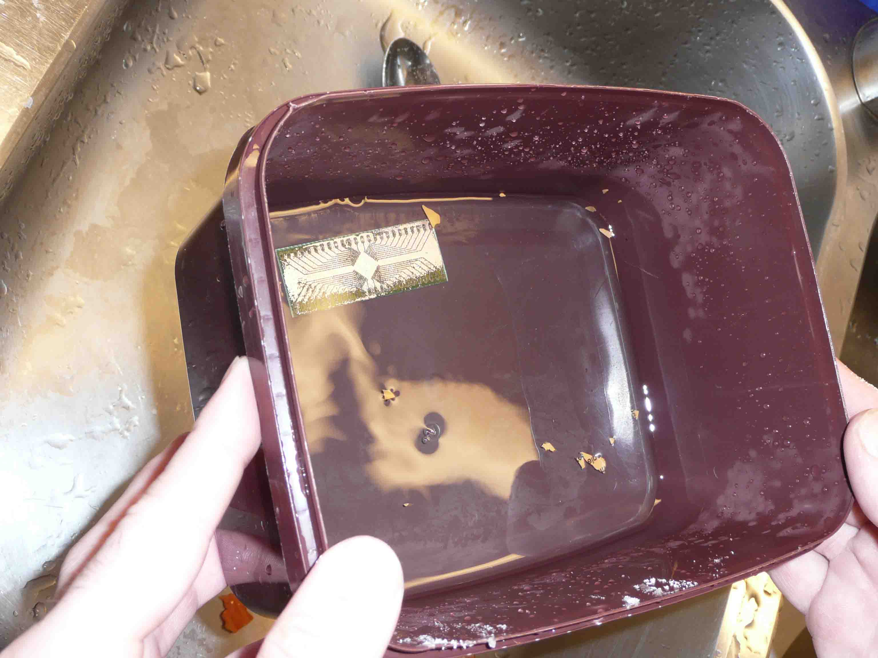
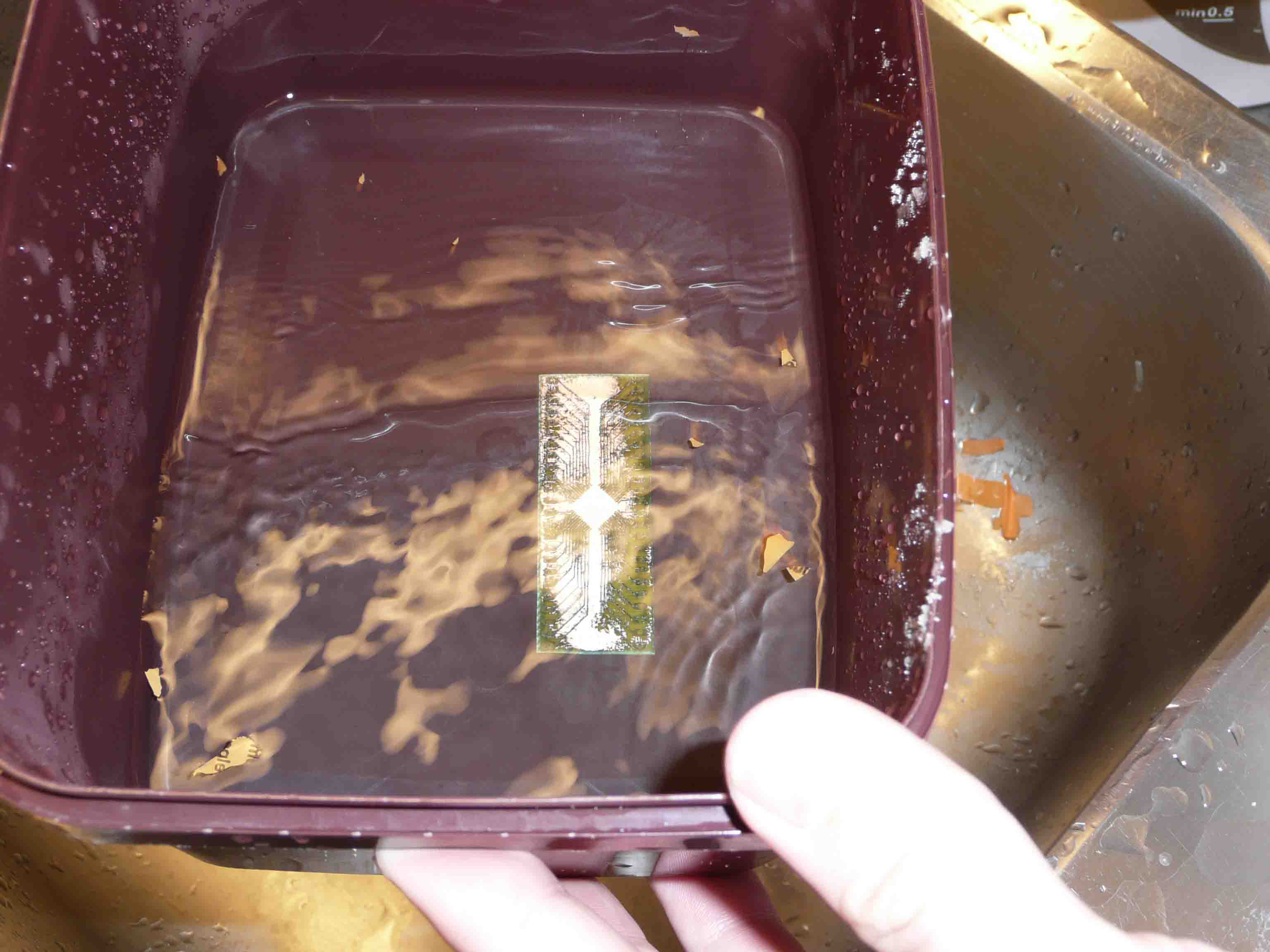
- If you get patches of "red-cupper" pour boiling water on the patches while still immersed in the etching-solution. This will convert the patches back to "white-cupper" patches, which you will be able to etch-away. (The red-cupper would have stayed).
- If you have trouble with cupper staying all over, maby the PCB is under-exposed, or under-developed.
- If you have trouble with traces being etched away, the film might not have been held against the laminate during exposure, or you have a not so good ink, or you developed to long? or you exposed to long(?). But the time window of ok exposure is usually pretty big (maby except for fine pitch), and the development you can see.
|